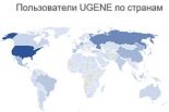
Юбилейный релиз UGENE 50.0 выпущен. В него вошли улучшения и обновления нескольких популярных инструментов – это Primer3 для подбора праймеров, база аннотаций для плазмид...
1 апреля наши сотрудники выступили на научном семинаре СУНЦ НГУ с лекцией «Современная биоинформатика c Unipro UGENE». Школьники 9-11 классов услышали о задачах, которые...
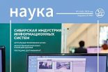
В конце ноября вышел в свет долгожданный ИТ-выпуск журнала СО РАН «Наука и технологии Сибири», посвященный наукоемким программным разработкам сибирских ученых и инженеров. Это...